- 您现在的位置:买卖IC网 > Sheet目录345 > MT42L256M32D4KP-3 IT:A (Micron Technology Inc)IC LPDDR2 SDRAM 8GBIT 168FBGA
�� �
�
�2Gb:� x16,� x32� Mobile� LPDDR2� SDRAM� S4�
�AC� Timing�
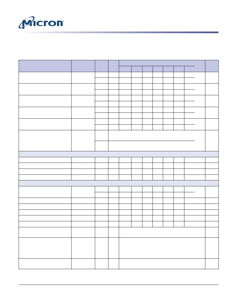
�Table� 86:� AC� Timing� (Continued)�
�Notes� 1–2� apply� to� all� parameters� and� conditions.� AC� timing� parameters� must� satisfy� the� t� CK� minimum� conditions� (in� mul-�
�tiples� of� t� CK)� as� well� as� the� timing� specifications� when� values� for� both� are� indicated.�
�Min/M� t� CK�
�Data� Rate�
�Parameter�
�Cumulative� errors� across� 8� cy-�
�cles�
�Cumulative� errors� across� 9� cy-�
�cles�
�Cumulative� errors� across� 10� cy-�
�cles�
�Cumulative� errors� across� 11� cy-�
�cles�
�Cumulative� errors� across� 12� cy-�
�cles�
�Symbol�
�t� ERR(8per),�
�allowed�
�t� ERR(9per),�
�allowed�
�t� ERR(10per),�
�allowed�
�t� ERR(11per),�
�allowed�
�t� ERR(12per),�
�allowed�
�ax�
�MIN�
�MAX�
�MIN�
�MAX�
�MIN�
�MAX�
�MIN�
�MAX�
�MIN�
�MAX�
�Min�
�–�
�–�
�–�
�–�
�–�
�–�
�–�
�–�
�–�
�–�
�1066�
�-217�
�217�
�-224�
�224�
�-231�
�231�
�-237�
�237�
�-242�
�242�
�933�
�-229�
�229�
�-237�
�237�
�-244�
�244�
�-250�
�250�
�-256�
�256�
�800�
�-241�
�241�
�-249�
�249�
�-257�
�257�
�-263�
�263�
�-269�
�269�
�667�
�-266�
�266�
�-274�
�274�
�-282�
�282�
�-289�
�289�
�-296�
�296�
�533�
�-290�
�290�
�-299�
�299�
�-308�
�308�
�-316�
�316�
�-323�
�323�
�400�
�-338�
�338�
�-349�
�349�
�-359�
�359�
�-368�
�368�
�-377�
�377�
�333�
�-362�
�362�
�-374�
�374�
�-385�
�385�
�-395�
�395�
�-403�
�403�
�Unit� Notes�
�ps�
�ps�
�ps�
�ps�
�ps�
�Cumulative� errors� across� n� =�
�t� ERR(nper),�
�MIN�
�t� ERR(nper),allowed,min�
�=� (1� +� 0.68ln(n))� �
�ps�
�13,� 14,� 15…,� 49,� 50� cycles�
�allowed�
�t� JIT(per),allowed,min�
�MAX�
�t� ERR(nper),�
�allowed,max� =� (1� +� 0.68ln(n))� �
�t� JIT(per),allowed,max�
�ZQ� Calibration� Parameters�
�Initialization� calibration� time�
�Long� calibration� time�
�Short� calibration� time�
�Calibration� RESET� time�
�t� ZQINIT�
�t� ZQCL�
�t� ZQCS�
�t� ZQRESET�
�MIN�
�MIN�
�MIN�
�MIN�
�–�
�6�
�6�
�3�
�1�
�360�
�90�
�50�
�1�
�360�
�90�
�50�
�1�
�360�
�90�
�50�
�1�
�360�
�90�
�50�
�1�
�360�
�90�
�50�
�1�
�360�
�90�
�50�
�1�
�360�
�90�
�50�
�μ� s�
�ns�
�ns�
�ns�
�READ� Parameters� 3�
�DQS� output� access� time� from�
�CK/CK#�
�t� DQSCK�
�MIN�
�MAX�
�–�
�–�
�2500�
�5500�
�2500� 2500� 2500� 2500� 2500� 2500�
�5500� 5500� 5500� 5500� 5500� 5500�
�ps�
�DQSCK� delta� short�
�t� DQSCKDS�
�MAX�
�–�
�330�
�380�
�450�
�540�
�670�
�900�
�1080�
�ps�
�4�
�DQSCK� delta� medium�
�t� DQSCKDM�
�MAX�
�–�
�680�
�780�
�900�
�1050� 1350� 1800� 1900�
�ps�
�5�
�DQSCK� delta� long�
�t� DQSCKDL�
�MAX�
�–�
�920�
�1050� 1200� 1400� 1800� 2400�
�–�
�ps�
�6�
�DQS-DQ� skew�
�Data-hold� skew� factor�
�t� DQSQ�
�t� QHS�
�MAX�
�MAX�
�–�
�–�
�200�
�230�
�220�
�260�
�240�
�280�
�280�
�340�
�340�
�400�
�400�
�480�
�500�
�600�
�ps�
�ps�
�DQS� output� HIGH� pulse� width�
�t� QSH�
�MIN�
�–�
�t� CH(abs)�
�-� 0.05�
�t� CK(a�
�vg)�
�DQS� output� LOW� pulse� width�
�t� QSL�
�MIN�
�–�
�t� CL(abs)�
�-� 0.05�
�t� CK(a�
�vg)�
�Data� half� period�
�t� QHP�
�MIN�
�–�
�MIN�
�(� t� QSH,� t� QSL)�
�t� CK(a�
�vg)�
�DQ/DQS� output� hold� time� from�
�t� QH�
�MIN�
�–�
�t� QHP�
�-� t� QHS�
�ps�
�DQS�
�PDF:� 09005aef83f3f2eb�
�2gb_mobile_lpddr2_s4_g69a.pdf� –� Rev.� N� 3/12� EN�
�143�
�Micron� Technology,� Inc.� reserves� the� right� to� change� products� or� specifications� without� notice.�
�2010� Micron� Technology,� Inc.� All� rights� reserved.�
�发布紧急采购,3分钟左右您将得到回复。
相关PDF资料
MT45W1MW16BDGB-708 AT
IC PSRAM 16MBIT 104MHZ 54VFBGA
MT48H32M16LFB4-75B IT:C
IC SDRAM 512MB 54VFBGA
MT48H8M16LFB4-75 IT:K TR
IC SDRAM 128MBIT 133MHZ 54VFBGA
MTC100-JA2-P34
CONTACT INSERT PIN
MX841BE
IC CONVERTER WHITE LED 8-SOIC
MXHV9910BTR
IC LED DRIVER HIGH BRIGHT 8-SOIC
MXN12FB12F
MOTOR BRUSHED DC 12V 2922RPM
MXN13FB08B1
MOTOR BRUSHED DC 8V 4714RPM
相关代理商/技术参数
MT42L256M32D4KP-MS
制造商:Micron Technology Inc 功能描述:256MX32 LPDDR2 PLASTIC IND TEMP GREEN WFBGA 1.2V - Bulk